The web hosting industry is highly competitive, dominated by large, established players. However, the foundational need for reliable web presence means there’s always room for a niche, customer-focused provider. The secret to starting a successful web hosting business with minimal investment lies in smart infrastructure choices and hyper-focused marketing.
Here is a step-by-step guide to building your hosting business without the high initial capital outlay.
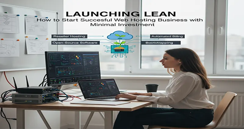
Phase 1: The Lean Start — Reseller Hosting
The single most critical decision for a low-investment start is choosing a Reseller Hosting model over purchasing or renting a Dedicated Server or VPS.
1. Embrace the Reseller Model
- What it is: You purchase a bulk amount of hosting resources (disk space, bandwidth, accounts) from a large, established provider at a wholesale rate and then divide and resell those resources under your own brand name.
- Minimal Investment: You avoid the massive costs and technical complexity of